The Atomic Force Microscopy Market 2025–2035: Market Size, Competitive Dynamics, and Forecast
GET A FREE SAMPLE
NEED A CUSTOM REPORT?
We can customize every report including purchasing stand-alone sections or country-level reports, as well as <b> offer affordable discounts for start-ups & universities.</b>
Share this report:


Introduction
Key Report Highlights
Dominant Segments
Competitive Intelligence
Strategic Insights
Regional Dynamics
Advancing Nanotechnology & Precision Measurement: Why Our Global Atomic Force Microscopy (AFM) Market Report is Essential for Next-Generation Scientific Innovation
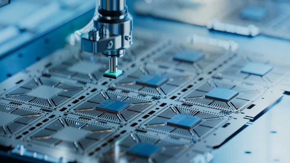
The global Atomic Force Microscopy (AFM) market is a highly specialized segment of the nanotechnology and analytical instrumentation industry, driven by rising demand for ultra-high-resolution surface characterization in semiconductor manufacturing, materials science, life sciences, and nanotechnology research. AFM enables imaging and measuring surfaces at the atomic and nanoscale level, making it essential for research institutions, industrial laboratories, and advanced manufacturing processes. With increasing investments in nanoscience, semiconductor miniaturization, and biotechnology, the market is witnessing steady global growth.
1. By Type: Industrial Grade AFM (Dominant Segment)
Industrial grade AFM holds the largest market share.
Why it dominates:
- High demand from semiconductor and electronics manufacturing
- Suitable for quality control and process monitoring
- High stability, automation, and repeatability
- Growing adoption in production environments
2. By Application: Semiconductors & Electronics (Dominant Segment)
Semiconductors and electronics lead the market.
Why:
- Critical for chip inspection and nanodevice development
- Supports miniaturization of electronic components
- Used in defect detection and surface analysis
- High R&D spending in advanced chip fabrication
3. By End-Use: Industrial Laboratories (Dominant Segment)
Industrial laboratories dominate usage.
Why:
- Strong demand for nanoscale quality assurance
- Integration into manufacturing workflows
- High adoption in materials testing and R&D
- Growing need for automated measurement systems
4. By Operation Mode: Dynamic Mode (Major Segment)
Dynamic (tapping) mode is widely used.
Why:
- Reduces damage to delicate samples
- Provides high-resolution imaging
- Suitable for biological and soft materials
- Increasing use in advanced research applications
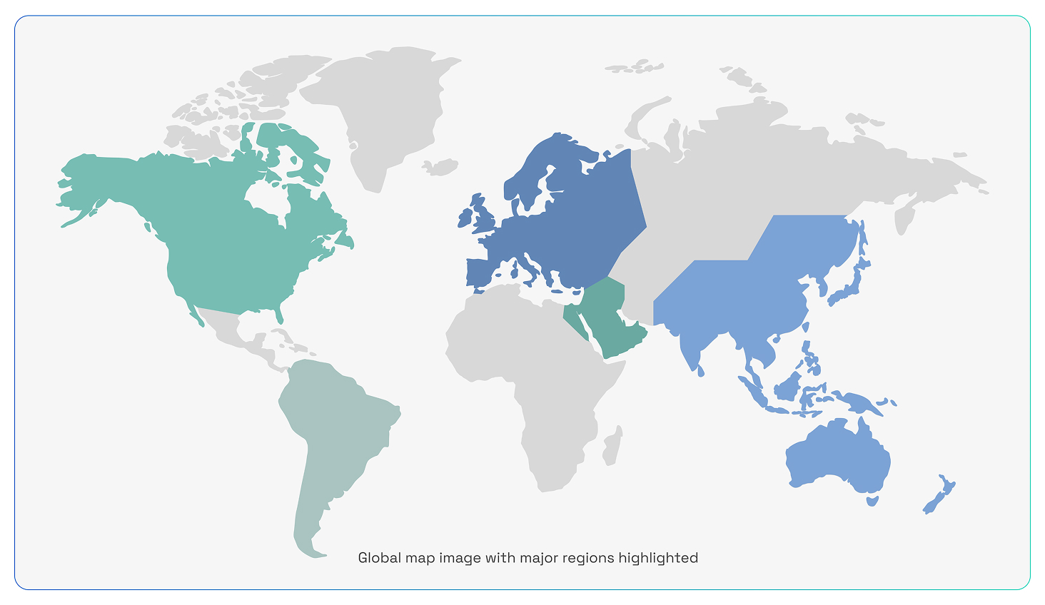
5. By Geography: North America (Dominant Region)
North America leads the global market.
Key factors:
- Strong semiconductor and nanotechnology R&D ecosystem
- High funding from academic and government institutions
- Presence of leading AFM manufacturers
- Advanced research infrastructure in universities and labs
Fastest-growing region:
- Asia-Pacific
Drivers: What is fueling market growth?
- Rising demand for nanoscale imaging and metrology
- Growth in semiconductor miniaturization and chip design
- Expanding nanotechnology and material science research
- Increasing adoption in life sciences and biomedical studies
- Advancements in automated and AI-enabled AFM systems
Restraints (R) – What is limiting growth?
- High cost of equipment and maintenance
- Need for skilled operators and technical expertise
- Complex sample preparation and analysis processes
- Limited throughput compared to other imaging techniques
Opportunities (O) – Where is future growth coming from?
- AI-driven AFM data analysis and automation
- Expansion in semiconductor fabrication and 2D materials
- Growth in biomedical and cellular imaging applications
- Development of high-speed and portable AFM systems
Trends (T) – What is shaping the future?
- Shift toward automated and high-throughput AFM systems
- Integration with machine learning and AI-based imaging
- Increasing use in real-time industrial quality control
- Growing demand for multi-mode and hybrid AFM technologies
Methodology
We use a stepwise research approach combining secondary research, primary validation, and data triangulation to estimate market size and forecast growth.
| Step | What we do |
|---|---|
| 1. Secondary research | Review public sources (company disclosures, industry publications, and credible datasets) to map the market and build baseline assumptions. |
| 2. Primary inputs | Validate assumptions through expert inputs (manufacturers, technology providers, and domain specialists). |
| 3. Sizing & forecasting | Apply structured sizing methods and forecast models using adoption trends, segment mix, and regional demand patterns. |
| 4. Triangulation | Cross-check estimates across multiple methods and sources to ensure consistency and reduce bias. |
Atomic Force Microscopy (AFM) Market: Core Overview
How Atomic Force Microscopy Is Advancing Nanoscale Research and Analysis
🔬 Key Applications
- Nanomaterials Research and Characterization
- Semiconductors and Electronics Testing
- Biological and Medical Imaging
- Surface Morphology and Material Science Studies
📈 Business Benefits
- High-Resolution Imaging at the Nanoscale
- Accurate Surface Topography and Measurements
- Supports Advanced R&D and Innovation
- Enables Precision in Material and Biological Analysis
⚙️ Core Technologies
- Scanning Probe Microscopy
- Piezoelectric and Feedback Control Systems
- High-Sensitivity Cantilever and Tip Designs
- Advanced Imaging and Data Analysis Software
Market Scope & Analysis
1. By Type
- Contact Mode AFM
- Non-Contact Mode AFM
- Tapping Mode AFM
- High-Speed AFM
2. By Application
- Material Science
- Semiconductors
- Life Sciences
- Nanotechnology
- Surface Analysis
3. By End-Use Industry
- Research Institutes
- Pharmaceuticals
- Electronics & Semiconductors
- Academic Institutions
- Industrial Laboratories
4. By Component
- AFM Systems
- AFM Probes
- Software
- Accessories
5. By Geography
- North America
- Europe
- Asia-Pacific
- Latin America
- Middle East & Africa
- Bruker
- Park Systems
- Oxford Instruments
- Nanosurf AG
- Hitachi High_Tech
- North America
- Europe
- Asia-Pacific
- Latin America
- Middle East
- Africa
- United States
- Canada
- Germany
- United Kingdom
- France
- China
- India
- Japan
- South Korea
- Australia
- Brazil
- Mexico
- United Arab Emirates
- Saudi Arabia
Recent Developments
Recent Developments
In January 2026, Bruker Corporation introduced its latest AFM platform featuring enhanced imaging resolution, faster scan rates, and advanced environmental controls for nanomechanical and materials research. The new system supports automated workflows and AI‑driven data analysis, enabling researchers in semiconductor, life sciences, and materials science to acquire higher‑fidelity data with greater throughput.
In October 2025, Oxford Instruments’ Asylum Research business unit launched a high‑speed AFM model optimized for biological and soft matter imaging, combining ultra‑fast scanning with low force interaction. This release enhances real‑time studies of molecular processes and improves imaging stability in liquid environments—appealing to academic and biotech research laboratories.
In August 2025, Park Systems announced the integration of AI‑based automation and analysis tools into its AFM controller software. The software enhancements support automated tip tuning, defect recognition, and pattern analysis, reducing operator setup time and improving reproducibility across nanometrology workflows in industrial R&D settings.
Frequently Asked Questions
A1: Atomic Force Microscopy Market is anticipated to grow at a CAGR of 8% in 2025 to 2035.
A2: The Atomic Force Microscopy Market is growing due to applications in nanotechnology research, materials science, semiconductor inspection, and biomedical analysis. Increasing adoption in academic and industrial research is driving demand globally.
A3: Top companies in the Atomic Force Microscopy (AFM) Market: Bruker Corporation, Park Systems, Oxford Instruments (Asylum Research), NT‑MDT Spectrum Instruments, Nanosurf AG, Hitachi High‑Tech Corporation.
A4: The main challenges hindering the adoption of the Atomic Force Microscopy Market include high equipment and maintenance costs, technical expertise requirements, and limited awareness among potential industrial and academic users.
A5: North America, Europe, and Asia Pacific (especially China and Japan), driven by growth in research & development, semiconductor inspection, materials science, and academic research applications.
A6: Key verticals in the Atomic Force Microscopy Market market include nanotechnology research, materials science, semiconductor industry, biomedical research, and academic institutions.
GET A FREE SAMPLE
This FREE sample includes market data points, ranging from trend analyses to market estimates & forecasts. See for yourself.
NEED A CUSTOM REPORT?
We can customize every report including purchasing stand-alone sections or country-level reports, as well as <b> offer affordable discounts for start-ups & universities.</b>
Share this report:
Seize Tomorrow's Opportunities Today: Access the Full Report
Our Top Selling Reports
- •Water-Soluble Vitamin & Mineral Feed Supplements Market
- •Pyridine & Pyridine Derivatives Market
- •Nutraceutical Ingredients Market
- •Functional Food Ingredients Market
- •Water-Soluble Vitamin & Mineral Feed Supplements Market
- •Pyridine & Pyridine Derivatives Market
- •Nutraceutical Ingredients Market
- •Functional Food Ingredients Market
Personalize This Report
- •Triangulate with your Own Data
- •Get Data as per your Format and Definition
- •Gain a Deeper Dive on a Specific Application, Geography, Customer or Competitor
- •Any level of Personalization
Let Us Help You
- •What are the Known and Unknown Adjacencies Impacting the Digital Health Market
- •What will your New Revenue Sources be?
- •Who will be your Top Customer; what will make them switch?
- •Defend your Market Share or Win Competitors
- •Customized Workshop Request